

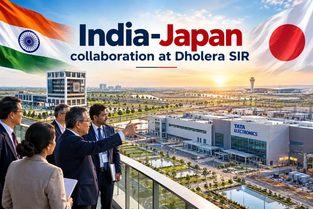
India’s semiconductor story is gathering pace, and Dholera Special Investment Region (SIR) in Gujarat is at the centre of it. A recent high-level visit from a Japanese delegation has added fresh momentum to this journey.
Mr. Kenji Hiramatsu, Former Ambassador of Japan to India (2015–2019), visited Dholera SIR to review the progress of its semiconductor ecosystem. He now serves as Chairman of The Institute for International Strategy at Japan Research Institute Limited, part of the SMBC Group.
He was accompanied by officials from the Japan Bank for International Cooperation (JBIC) and the National Industrial Corridor Development Corporation (NICDC). For anyone watching Dholera’s growth, this visit sends a clear signal: global partners are paying close attention.
At Angel Nova, we track developments like these closely because they shape the long-term value of the region. Here is a detailed look at the visit and why it matters.
Why Japan’s Role in India’s Semiconductor Mission Matters
Japan is one of the world’s most respected names in advanced manufacturing, electronics, and precision engineering. Its expertise in semiconductor materials, equipment, and supply chains is widely recognised.
India, on the other hand, is building its semiconductor capacity almost from the ground up. It needs technology partners, investment, and proven know-how.
This makes the India-Japan partnership a natural fit. Japan brings experience and capital. India brings scale, talent, land, and strong government support.
Engagements between Japanese administration, industry leaders, and Indian authorities have been growing steadily. Dholera SIR has emerged as a key meeting point for this collaboration.
Inside the Visit: What the Delegation Reviewed
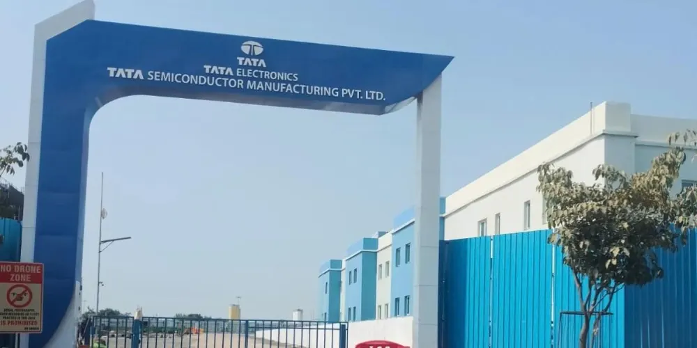
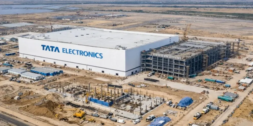
During the visit, Mr. Hiramatsu reviewed recent developments across Dholera SIR. A key focus was the progress of the semiconductor fabrication facility being developed by Tata Semiconductor Manufacturing Private Limited.
This is India’s first semiconductor fabrication plant, often called a “fab.” Its presence alone has put Dholera on the global technology map.
The delegation was welcomed by Ms. Amita Pargi, GAS, General Manager – Land & Municipal Services at Dholera Industrial City Development Limited (DICDL), along with other officials.
The group toured several key facilities, including:
- The Administrative Building, which serves as the administrative hub of the city.
- The Command and Control Centre, housed within the City Integrated Operations Centre at the ABCD Building.
- Integrated water and power infrastructure inside the Activation Area.
Officials from DICDL briefed the delegation on Dholera’s strategic location, multimodal connectivity, trunk infrastructure, and plug-and-play facilities built for large-scale investment.
A Complete Ecosystem, Not Just a Factory
One of the most important takeaways from the visit is that Dholera is not just building a single plant. It is building an entire ecosystem around it.
Alongside the semiconductor fab, Dholera is developing industrial, residential, and commercial infrastructure at the same time. This approach is designed to meet the changing needs of the semiconductor industry.
A fab needs far more than a building. It needs reliable power, large volumes of clean water, skilled workers, housing, schools, healthcare, and logistics support.
Dholera’s planners have built these needs into the city’s foundation. This is what makes the region attractive to global companies looking for a long-term base in India.
The Smart City Backbone: Command and Control Centre
The City Integrated Operations Centre at the ABCD Building is one of Dholera’s standout features. It acts as the brain of the smart city.
From here, officials can monitor and manage essential city services in real time. This includes utilities, traffic, security, and emergency response.
For global investors, especially from technology-driven nations like Japan, this level of digital city management is reassuring. It shows that Dholera is being built with modern governance and efficiency in mind.
Semiconductor manufacturing depends heavily on stable operations. Even a short power cut or water disruption can cause major losses. A centralised control system helps reduce these risks.
Infrastructure Built for Scale
Dholera’s plug-and-play model is designed to help companies set up operations faster. Instead of spending years arranging land, utilities, and approvals, investors can move into ready infrastructure.
The Activation Area already features integrated water and power systems. Trunk infrastructure such as roads, drainage, and utility networks is being developed in a planned manner.
Connectivity is another strong point. The region is supported by expressway, rail, air, and port links, giving businesses easy access to domestic and international markets.
This combination of readiness and connectivity is exactly what large-scale manufacturers look for.
What This Visit Means for Dholera’s Future
High-level visits like this one are more than ceremonial. They often lead to deeper conversations about investment, partnerships, and funding.
The presence of JBIC officials is especially notable. JBIC is Japan’s policy-based financial institution and has supported major infrastructure and industrial projects across the world.
NICDC’s involvement reflects the Indian government’s commitment to developing Dholera as a flagship industrial corridor city.
Together, these institutions signal confidence in Dholera’s direction. As more global partners engage with the region, demand for industrial, commercial, and residential space is likely to grow.
Why Investors Are Watching Dholera Closely
Dholera is steadily moving from vision to reality. The semiconductor fab, smart city systems, and growing international interest are all visible signs of progress.
For investors and homebuyers, early-stage growth regions often present opportunities before they become mainstream. As industry arrives, jobs follow. As jobs grow, housing and commercial needs increase.
At Angel Nova, we believe that understanding these developments is essential for making informed decisions. Every major announcement, visit, and infrastructure milestone adds another layer to Dholera’s story.
That said, every investment should be made with careful research, verified documentation, and a long-term view.
Conclusion
The visit of Mr. Kenji Hiramatsu and the Japanese delegation marks another important step in strengthening India-Japan collaboration at Dholera SIR.
With India’s first semiconductor fab taking shape, world-class infrastructure in place, and global partners showing strong interest, Dholera is positioning itself as a future hub for high-tech manufacturing.
For those who want to be part of this growth story, now is the time to stay informed. Follow Angel Nova for the latest updates on Dholera SIR, its infrastructure, and the opportunities it brings.
Frequently Asked Questions
He is the Former Ambassador of Japan to India (2015–2019) and currently Chairman of The Institute for International Strategy at Japan Research Institute Limited, part of the SMBC Group.
The visit aimed to review the development of Dholera’s semiconductor ecosystem, including the Tata semiconductor fab and supporting infrastructure.
The delegation included officials from JBIC (Japan Bank for International Cooperation) and NICDC (National Industrial Corridor Development Corporation).
Tata Semiconductor Manufacturing Private Limited is developing India’s first semiconductor fabrication plant at Dholera SIR.