

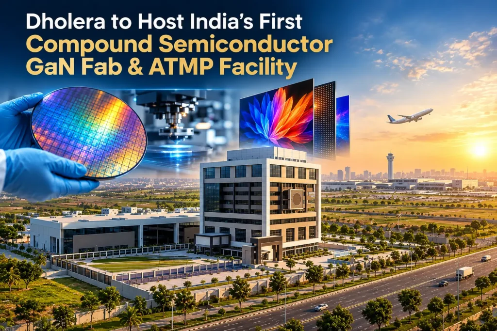
Dholera is no longer just a city on a master plan. It is fast becoming India’s semiconductor address.
The Union Cabinet has approved Crystal Matrix’s project under the Compound Semiconductor Scheme of the India Semiconductor Mission (ISM). With this, the Dholera semiconductor fab story gets a powerful new chapter: India’s first compound semiconductor Gallium Nitride (GaN) fab and ATMP facility for the Mini/Micro-LED ecosystem.
At Angel Nova Group, we track every development shaping Dholera Special Investment Region (SIR). This one is a big deal. Here is everything you need to know.
1. What Has Been Approved in Dholera?
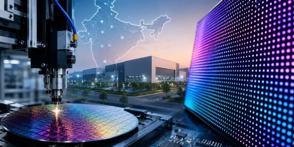
Crystal Matrix will set up a compound semiconductor GaN fabrication unit along with an ATMP (Assembly, Testing, Marking and Packaging) facility in Dholera SIR.
The project has been approved under the Compound Semiconductor Scheme of ISM. It is the first facility of its kind in India, focused on GaN technology and next-generation display panels.
Project at a glance:
| Parameter | Details |
| Company | Crystal Matrix |
| Scheme | Compound Semiconductor Scheme, India Semiconductor Mission |
| Investment | ₹3,068 crore |
| Land allotted | 40 acres in Dholera SIR |
| Products | Mini/Micro-LED display panels, GaN epitaxy wafers |
| Annual capacity | 24,000 sets (each) of RGB GaN wafers and 72,000 sq. m of Mini/Micro-LED display panels |
| Direct jobs | 1,600+ |
This is a clear signal that Dholera is being positioned as a full-spectrum semiconductor hub, not a single-project town.
2. Why GaN and Mini/Micro-LED Technology Matter
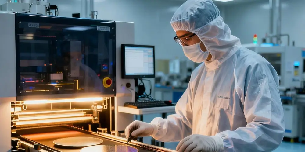
Most people have heard of silicon chips. Compound semiconductors are different. They are made by combining two or more elements, and Gallium Nitride is one of the most important among them.
GaN handles high power, high frequency and high temperatures far better than conventional silicon. That makes it valuable for fast chargers, electric vehicles, 5G equipment, defence electronics and, importantly, LED lighting and displays.
Mini-LED and Micro-LED displays are the next step after OLED. They offer brighter screens, deeper contrast, longer life and better energy efficiency. You will find them in premium TVs, smartwatches, AR/VR headsets, automotive dashboards and large outdoor displays.
Until now, India has depended heavily on imports for these components. A domestic GaN fab changes that equation.
3. The ₹3,068 Crore Investment: What It Will Produce
The investment of ₹3,068 crore will strengthen India’s manufacturing capabilities in compound semiconductors and advanced display technologies.
The facility will produce two core product lines:
- GaN epitaxy wafers – the base material on which GaN chips and LEDs are built. Annual capacity: 24,000 sets of RGB GaN wafers.
- Mini/Micro-LED display panels – finished display modules. Annual capacity: 72,000 square metres.
By covering both wafer production and panel assembly, the project builds a complete value chain within one campus. That reduces import dependence and creates room for local suppliers to grow around it.
4. 1,600+ Direct Jobs and a Skilled Workforce
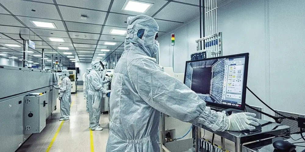
Beyond the technology, the project is expected to generate more than 1,600 direct jobs.
These are high-skill roles in process engineering, cleanroom operations, quality testing, equipment maintenance and packaging. Every such job also supports indirect employment in logistics, housing, retail, hospitality, education and healthcare.
For Dholera, this means a growing resident population of engineers, technicians and professionals. People who work in Dholera will want to live near Dholera. That is where real, long-term demand begins.
5. How This Strengthens Dholera as a Semiconductor Hub
The Crystal Matrix approval does not stand alone. Dholera SIR already hosts India’s first commercial semiconductor fab being developed by Tata Electronics, announced under the ISM.
Now, with a compound semiconductor GaN fab joining the ecosystem, Dholera is attracting both silicon and compound semiconductor manufacturing. Industries like these tend to cluster. Once anchor units arrive, component makers, chemical and gas suppliers, equipment vendors and service providers follow.
Dholera’s advantages make this clustering possible:
- Planned, greenfield city with plug-and-play infrastructure
- Dedicated activation area with trunk roads, power and water systems
- Ahmedabad–Dholera Expressway improving connectivity
- Upcoming Dholera International Airport
- Strong policy support from the Government of Gujarat and the Centre
Each new approval adds credibility. Each project makes the next one easier to attract.
6. What It Means for Dholera Real Estate and Investors

Industrial growth is one of the strongest drivers of real estate demand. When large manufacturing units bring thousands of jobs, the need for housing, commercial spaces and social infrastructure rises steadily.
For investors, the Dholera semiconductor fab developments point to a few clear trends:
- Residential demand from employees, contractors and their families
- Commercial opportunities such as shops, offices, hotels and service centres
- Infrastructure-led appreciation as roads, utilities and connectivity improve
- Long-term confidence backed by government-approved, high-value projects
That said, smart investing is about choosing the right location and the right partner. Plots with clear titles, proper approvals and proximity to key infrastructure are what matter most.
This is where Angel Nova Group helps. We guide investors with verified projects, transparent documentation and on-ground knowledge of Dholera SIR.
7. The Bigger Picture: A Self-Reliant Semiconductor India
India’s semiconductor mission is about more than factories. It is about securing supply chains, reducing imports and building strategic technology capability at home.
The Crystal Matrix project marks another step towards a resilient and self-reliant semiconductor ecosystem. Compound semiconductors, in particular, are critical for defence, telecom, energy and consumer electronics.
Dholera sits at the heart of this national vision. As more fabs, ATMP units and suppliers choose Dholera, the city’s identity as India’s semiconductor capital grows stronger.
For anyone watching Dholera’s journey, this is the time to pay attention.
Conclusion
The approval of India’s first compound semiconductor GaN fab and ATMP facility in Dholera SIR is a milestone for the country and for the city. A ₹3,068 crore investment, 40 acres of land, advanced Mini/Micro-LED products and 1,600+ direct jobs together send a strong message: Dholera is ready for the future.
Want to explore investment opportunities in Dholera SIR? Connect with Angel Nova Group today for verified projects, expert guidance and complete transparency.
Frequently Asked Questions (FAQs)
Crystal Matrix, under the Compound Semiconductor Scheme of the India Semiconductor Mission.
The project involves an investment of ₹3,068 crore.
40 acres in Dholera Special Investment Region (SIR).
Mini/Micro-LED display panels and GaN epitaxy wafers.